Difference between revisions of "FTDI ATmega"
(→pinout) |
|||
| Line 47: | Line 47: | ||
* led2 is connected to CBUS0 (FT232RL) PC -> AVR activity |
* led2 is connected to CBUS0 (FT232RL) PC -> AVR activity |
||
* led3 is connected to CBUS1 (FT232RL) AVR -> PC activity |
* led3 is connected to CBUS1 (FT232RL) AVR -> PC activity |
||
* led4 is connected to |
* led4 is connected to PC4 |
||
* led5 is connected to |
* led5 is connected to PC5 |
||
=== Arduino Pinout === |
=== Arduino Pinout === |
||
Revision as of 15:22, 17 January 2012
FTDI-atmega
This is the documentation page for the FTDI-atmega PCB. which can be purchased here: http://www.bitwizard.nl/catalog/product_info.php?products_id=29
overview
The FTDI-atmega PCB has an USB connector and a 20-pin IO connector. The brains of the PCB is an ATmega168 chip.
Assembly instructions
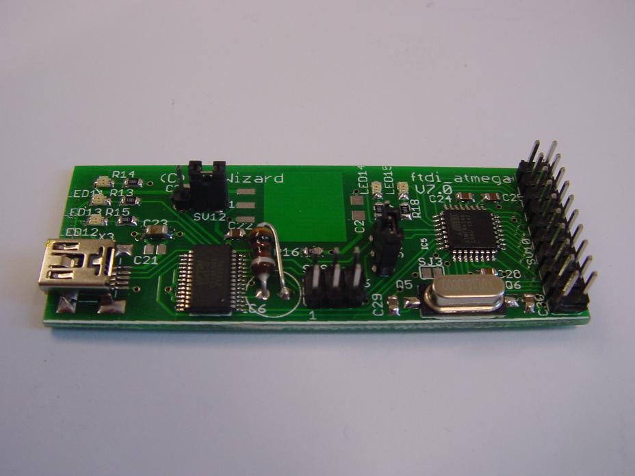
Nothing to be done, the module comes completely assembled, as in the picture below:

External resources
pinout
The 20 pin connector is connected as follows
| 1 | GND |
| 2 | GND |
| 3 | PC3 |
| 4 | PC2 |
| 5 | PC1 |
| 6 | PC0 |
| 7 | PB5 |
| 8 | PB4 |
| 9 | PB3 |
| 10 | PB2 |
| 11 | PB1 |
| 12 | PB0 |
| 13 | PD7 |
| 14 | PD6 |
| 15 | PD5 |
| 16 | PD4 |
| 17 | PD3 |
| 18 | PD2 |
| 19 | VCC |
| 20 | VCC |
- led1 is connected to VCC (the top one, called led2 on V7.0)
- led2 is connected to CBUS0 (FT232RL) PC -> AVR activity
- led3 is connected to CBUS1 (FT232RL) AVR -> PC activity
- led4 is connected to PC4
- led5 is connected to PC5
Arduino Pinout
When using the Arduino IDE, the layout of the header is as follows:
| GND | GND |
| A3 | A2 |
| A1 | A0 |
| 13 | 12 |
| 11 | 10 |
| 9 | 8 |
| 7 | 6 |
| 5 | 4 |
| 3 | 2 |
| V+ | V+ |
- Unlike a regular arduino, the onboard LED is connected to pin A5. This means pin 13 is free for regular use.
- Pin 0 and 1 are used for the COM interface just like a regular arduino.
- Pin 3, 5, 6, 9, 10 and 11 support PWM (analogWrite), just like a regular arduino.
Jumper settings
SV1 (next to the AVR): ICSP-Enable. CAUTION! Pin 1 and 2 are connected by a narrow PCB track. Cut this if you want to change this jumper setting.
1-2: ICSP enabled, SS connected to reset (programming the MCU over the 6-pin connector is enabled)
2-3: Default: SS connected to pin PB0 (MCU can function as an SPI slave or master, or as an ICSP programmer)
SV4 (next to the LEDs): Power supply selection.
No jumper: 3V3 > 90mA, extra regulator needs to be mounted.
1-2: Runs on 5V from USB
2-3: Runs on 3V3 from the FTDI chips internal regulator.
programming
This section describes how you get your program into the processor.
Linux
You can program the processor using any ICSP programmer that you might have. In that case, the jumper SV1 should then be in the upper position (away from the ICSP connector).
Or you can program it with the ftdi bitbang programmer included on the board.
Here is the documentation: http://www.geocities.jp/arduino_diecimila/bootloader/index_en.html
The ftdi-bitbang programmer-driver for avrdude is not included in the standard avrdude program. The reason is that the patch uses the ftdi library FTD2xx and not the open source libftdi.
In the avrdude bug tracking system another patch is doing the rounds, but that one is really slow because it doesn't exploit the ftdi's synchronous mode.
A precompiled avrdude version can be downloaded here: http://www.bitwizard.nl/avrdude.zip . The zipfile contains "quick and dirty" instructions to replace the avrdude binary in /usr/bin with a script so that when "arduino IDE" calls it, the program gets programmed into the board.
TODO: port the fast ftdi bitbang code to libftdi and submit to avrdude.
windows
See the linux section above.
writing programs
The chip is an ATmega168. http://www.atmel.com/dyn/resources/prod_documents/doc2545.pdf
future hardware enhancements
Provide a 3- or 4-pin header with the i2c pins (to communicate with wiimote and other peripherals). The leds need to be disabled for this to work. :-(
future software enhancements
- Add a reset button
Changelog
7.1
- Added decoupling capacitor for FTDI 3.3
- Added SJ for arduino compatibility.
b7.0
- Initial public release
